LS Note 170: Pulsed Power Supply for Three APS Septum Magnets
LS Note 170
Pulsed Power Supply for Three APS Septum Magnets
D. G. McGhee
March 24, 1991
Table of Contents
Abstract
Introduction
Switching Circuits
Controlled Charging-Choke Circuit
Warning
Pulsing Directly Into the Load
Simulation Results
Control and Interlock Logic
References
Three septum magnets will be operated at a repetition-rate of 2 Hz. Two of the septum magnets are identical and operate at the same values; these are the synchrotron extraction and the storage ring injection magnets. They are transformer septum magnets, with a primary inductance of 23 µH and resistance of 6.3  , and must be pulsed at a 2 Hz rate to extract beam from the synchrotron and inject beam into the storage ring at 7.7 GeV. The third septum magnet is used to inject electrons into the synchrotron at 650 MeV or positrons at 450 MeV. It is also a transformer septum magnet, with a primary inductance of 21 µH and resistance of 6.7 , and must be pulsed at a 2 Hz rate. A design study was performed of the power supply proposed in the APS Title I design. This supply produces a pulse that is approximately a half-sine-wave with a base width of approximately 1/3 ms; its peakcurrent is adjustable from 470 A to 4.7 kA and is repeatable within ±0.05%. The septum steel is reset by a half-sine pulse of reverse polarity a few milliseconds after the forward current pulse. No beam is present during reset. The use of the transformer design minimizes the cost of the capacitors used for energy storage.
Introduction
The septum magnets could be operated dc from a beam perspective. If they were operating dc the current leads would be required to be 47 to 63 times as large and the power loss in the magnet would be 2209 to 3969 times the pulsed operation, this would increase the power density in the septum edge to a level that would result in unacceptable operating temperature.
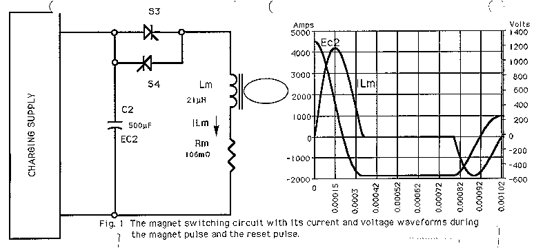
During the injection of the 650 MeV electron or 450 MeV positron beam from the Linac or PAR into the Synchrotron the septum magnet will be pulsed. Also, during extraction of the 7.7 GeV electron or positron beam from the Synchrotron and the injection into the Storage Ring, 3 septum magnets will be used for each function, 2 are dc and 1 is pulsed. All 3 pulsed septum magnets have approximately the saem rise and fall time. The septum's current pulse is required to be < 1 ms and the flattop time > 1 µs. These requirements are met with a capacitor discharge circuit that is resonant with the septum magnet at a frequency of approximately 1500 Hz. The peak current for the Synchrotron injection septum is 4227 A in the transformer primary and 16888 A in the secondary. The other 2 pulsed septums are identical and operate at approximately the same required current of 3800 A in the transformer primary and 11400 A in the secondary. These requirements can also be met with a half sinewave pulse. This is accomplished by discharging the energy stored in capacitor bank (C2) into the magnet as illustrated by Fig. 1. On triggering the forward thyristor S3 the energy stored in C2 between pulses is discharged into the magnet circuit. S3 turns off at the end of the first half cycle of the damped oscillation. C2 is then left with a smaller charge of opposite polarity until the reverse thyristor S4 is triggered and the second half cycle takes place with current flowing in the opposite direction. The difference between the original and the final charge is furnished by the charging supply between septum pulses.
The switching circuits of these 3 septums operate in the same way as the injection/extraction septum for PAR. [1] Whne the capacitor, C2, of Fig. 1 is discharged into the load, an oscillatory current will result provided that the total resistance in the circuit is sufficiently low.
The resonant frequency of the circuit is:
fr = ß/2                          [sd-1]     (1)

where ß = ((1/LMC2)-(Rm2/4Lm2))0.5         [s-1]
[sd-1] (1)
where ß = ((1/LMC2)-(Rm2/4Lm2))0.5 [s-1]
C2 = capacitor bank [F]
Lm = total circuit inductance [H]
Rm = total circuit resistance [ ]
]
The current at any time is:
i = (E/ßLm)e- t sin ßt [A] (2)
where t = time after discharge starts [s]
t sin ßt [A] (2)
where t = time after discharge starts [s]
= RM/2 Lm [s-1]
The required voltage on C2 for the different peak operating currents is:
EC2 = ißLm/e-t sin ßt [V] (3)
These values are shown in Table 1 for each of the 3 magnets operating at 2 different energies.
The time at which the current reaches its first peak is:
tp = 1/ß tan-1 ß/ [s] (4)
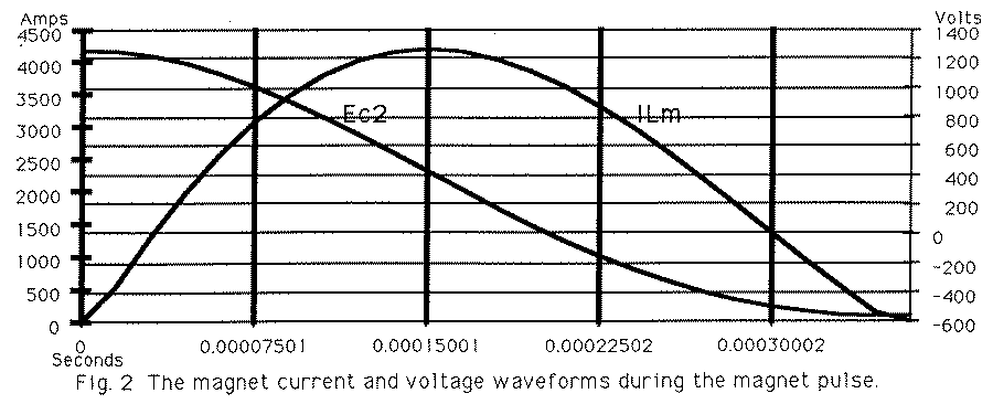
The first current peak does not occur at precisely the first quarter period of the discharge cycle, but at a previous point in time. This is shown by the circuit simulation graphed in Fig. 2. The term tan-1ß/ describes the phase angle at which the peak current occurs.
In this application, Rm is made appreciably less than the value for critical damping. With 1/LmC2 > Rm2/4 Lm2 we can write ß  1/(LmC2)0.5 and the above equations can be simplified to:
	fr  1/(2(LmC2)0.5)                [s-1]      (1')

	i  EC2(C2/Lm)0.5e-tsin t/(LmC2)0.5 [A]        (2')

The peak current is then

	Ip  EC2(C2/Lm)0.5 e-((Rm/4)(C2/Lm)0.5)[A]        (2'')

and the voltage on the first reversal becomes

	EC2  -EC2 e-((Rm/2)(C2/Lm)0.5)       [V]        (5)

Critical damping occurs at a resistance:

	Rm = 2(Lm/C2)0.5                     []       (6)
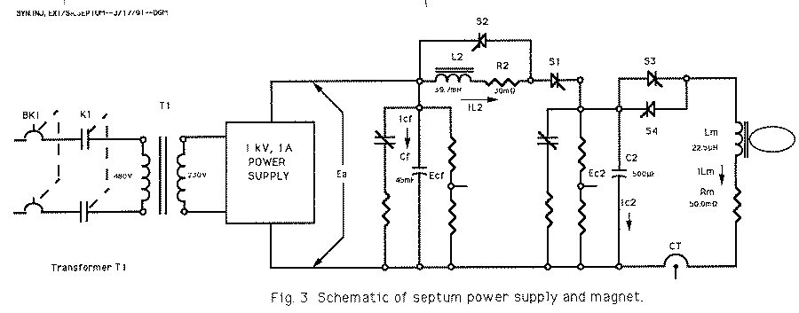
Fig. 3 shows the controlled charging-choke circuit and the capacitor discharge circuit of Fig. 1 combined. The discharge capacitor C2 is charged and recharged to make up the circuit losses incurred in pulsing the magnet. These losses are made up from a commercial 1 kW regulated dc power supply, PS1, and a capacitor bank, Cf. PS1 has constant voltage and constant current mode of operation with automatic crossover. This allows the direct connection to Cf, as PS1 will operate in the constant current mode until crossover occurs at the output voltage set point. The key power supply specifications are given in Table 2. The capacitor bank Cf is used to allow the losses to be made up at a fixed time before the next pulse of the main switching circuit. The controlled charging circuit consists of L2, C2, S1 and S2. Gating on of S1 is used to start the charging of C2 from the dc power supply. At time t0 the supply voltage E begins to drive an essentially sinusoidal current through the charging circuit.
E = iR2 + L2(di/dt) + (1/C)  iC2 dt (8)
At time t1 the current is at its peak and
	L2 di/dt = 0,                             (9)


	E = iR2 + (1/C2  iC2 dt.                (10)
Between t1 and t2 the decaying charging current generates a voltage L2 (di/dt) which aids the supply voltage to charge the capacitor C2 to a voltage larger than E. In the case where R => 0, this voltage will be, at time t2
ec2 = E + L (di/dt) = 2E.
By providing a thyristor across the charging choke as shown in Fig. 3 the charging cycle can be terminated at any instant between times t1 and t2. A fraction of the capacitor voltage eC2 is compared with a reference voltage. At time tr when the capacitor voltage is  the supply voltage, a pulse can be generated which turns on S2. With S2 conducting, the driving voltage L2 (di/dt) is removed from the circuit and the capacitor voltage eC2 is larger than the power supply voltage E, thyristor S1 is back-biased and the charging current iC2 stops. The current iL2 flowing in choke L2 at time tr will decay with a time constant L2/R2, where R2 is the resistance of the choke and thyristor, S2, circuit. Thyristor S2 remains on until the time S1 is gated on starting the charge cycle again, or the choke current decays to 0. The current iL2 flowing in the choke when S2 is turned off will aid in charging capacitor C2 (the energy 0.5 L2 iL22 is returned to the circuit). This makes the circuit very efficient.
It should be noted that the Q of the discharge circuit in Fig. 1 should be < 5 for this charging circuit to operate properly. As the Q increases the current flowing in the choke L2 will decrease. This in turn decreases the operating range of the charging circuit.
Heat losses in the magnet can be cut by approximately 1/3 and the circuit efficiency can be increased by not gating S4, and resetting the required output voltage of PS1.
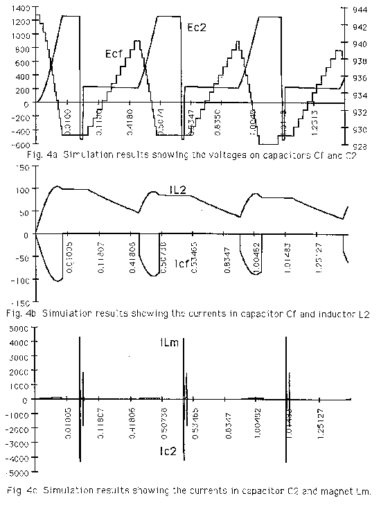
Two septum circuits with 2 beam energies per circuit were simulated with the magnets each having a Q of 2. The charge voltages used are given in Table 1. The peak and rms voltages/currents for all the pulsed septum magnets operating at 2 Hz and the waveforms for the synchrotron injection septum power supply at the different circuit nodes, are shown in Fig. 4 a, b and c. These simulations were done using a piecewise simulation program. [2] The simulated waveforms have a varied time axis so that they show in detail what happens during the charge and discharge of C2.
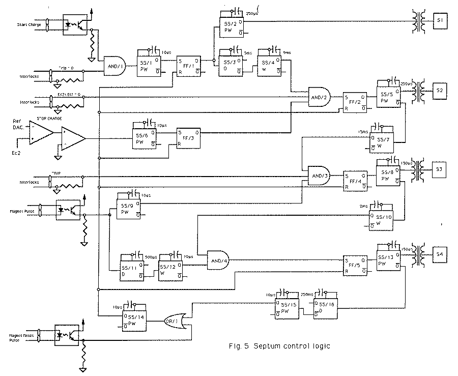
Control and Interlock Logic
Control logic is shown in Fig. 5. Control is accomplished with 3 gate pulses from the power supply control unit (PSCU) or a master clock and 3 interlock signals from the interlock circuit.
The "Start Charge" pulse is optically coupled to AND/1 with a signal from the interlock trip circuit. When the trip signal is low the power supply is completely shutoff and crowbarred. When both the "Start Charge" pulse and the interlock are logic 1s then the AND's output is true (1) setting the flip-flop, FF/1, causing single shot, (SS)/2's Q output to go high and stay there for 250 µs. This pulse is amplified and coupled with the pulse transformer to gate Thyristor S1. This starts the resonant charge of C2 from Cf through L2, as shown in Fig. 4.
At the time SS/2 is triggered, SS/3 is also triggered, which causes its q/not output to go low. The pulse width of SS/3 is 5 ms and at the end of this pulse Q/not goes high triggering SS/4. The Q output pulse of SS/4 is 9 ms and is used as a window during which time Ec2 is compared to the DAC voltage and Ec2 is also compared with Ecf in the interlock circuit. If Ec2 is greater than both voltages, Ecf, and the DAC then all 3 inputs to AND/2 are 1s. This causes the AND's output to be true (1) setting the flip-flop, FF/2, causing single shot, (SS)/5's Q output to go high and stay there for 250 µs. This pulse is amplified and coupled with the pulse transformer to gate Thyristor S2. This stops the resonant charge of C2 by crowbarring L2, as shown in Fig. 4.
At the end of the SS/5 Q output pulse SS/7 is triggered causing a Q output pulse of SS/7. The pulse is 15 ms and is used as a window during which time, as long as the trip circuit is satisfied, a "Magnet Current" pulse can wide. This causes the AND's output to be true (1) setting the flip-flop, FF/4, causing single shot, (SS)/8's Q output to go high and stay there for 150 µs. This pulse is amplified and coupled with the pulse transformer to gate Thyristor S3. This starts the resonant current pulse of Lm by discharging C2 and recharging with the other polarity, as shown in Fig. 2.
At the end of the SS/8 Q output pulse SS/10 is triggered causing a Q output pulse. Also at the time the "Magnet Current" pulse SS/11 is also triggered causing its Q/not output to go low. The pulse width of SS/11 is 0.5 ms and at the end of this pulse Q/not goes high triggering SS/12. The Q output pulse of SS/12 is 10 µs wide and is used to cause the AND's output to switch to true (1) setting the flip-flop, FF/5, causing single shot, (SS)/13's Q output to go high and stay there for 150 µs. This pulse is amplified and coupled with pulse transformer to gate Thyristor S4. This starts the resonant current pulse of Lm by discharging C2 and recharging with the other polarity, as shown in Fig. 1. The current pulse resets the magnet core.
At the end of the SS/13 Q output pulse SS/16 causes its Q/not output to go low. The pulse width of SS/16 is 250 ms and at the end of this pulse Q/not goes high triggering SS/15. The Q output pulse of SS/15 is 10 µs and is ORed with a "Magnet Reset" pulse. Either pulse will reset all flip/flops (FF) with a 10 µs pulse from SS/14.
References
- D. G. McGhee, "Pulsed Power Supply for PAR Injection/Extraction Septum Magnet," ANL Light Source Note, LS-159, September 23, 1990.
- D. E. Piccone, I. L. Somos, and W. H. Tobin, "Piecewise Simulation (PS) Computation Method for Computing Transient Phenomena," IEEE-IAS Annual Meeting, September 1975, Page 326-331.
Table 1 APS's 2 Hz septum systems operating voltages and currents
| Description |
| Machine | Synchrotron | Synchrotron | Synchrotron | Synchrotron | Storage Ring | Storage Ring |
| Septum | Injection | Injection | Extraction | Extraction | Injection | Injection |
| Energy | 650 MeV | 450 MeV | 7.7 GeV | 7 GeV | 7.7 GeV | 7 GeV |
| Peak Primary Current | 4227 | 2926 | 3800 | 3455 | 3800 | 3455 |
| Primary Magnet Inductance | 0.000021 | 0.000021 | 0.000023 | 0.000023 | 0.000023 | 0.000023 |
| Capacitor Voltage C2 [Ec2.Q | 1258 | 871 | 1166 | 1060 | 1166 | 1060 |
| PS1 Voltage | 944 | 653 | 874 | 795 | 874 | 795 |
| Simulation |
| Voltages | |
| Ecf--{max}peak | 943 | 653 | 874 | 795 | 874 | 795 |
| Ecf--{min}peak | 928 | 643 | 861 | 783 | 861 | 783 |
| Ecf--rms | 934 | 650 | 868 | 790 | 868 | 790 |
| Ec2--{max}peak | 1258 | 871 | 1166 | 1060 | 1166 | 1060 |
| Ec2--{min}peak | -537 | -371 | -518 | -471 | -518 | -471 |
| Ec2--rms | 288 | 198 | 280 | 254 | 280 | 254 |
| Currents | |
| Icf--{max}peak | 1 | 1 | 1 | 1 | 1 | 1 |
| Icf--{min}peak | -105 | -72 | -97 | -88 | -97 | -88 |
| Icf--rms | 10 | 7 | 9 | 8 | 9 | 8 |
| Ic2--{max}peak | 1849 | 1279 | 1732 | 1575 | 1732 | 1575 |
| Ic2--{min}peak | -4322 | -2990 | -3888 | -3535 | -3888 | -3535 |
| lc2--rms | 91 | 63 | 84 | 77 | 84 | 77 |
| ILm--{max}peak | 4321 | 2989 | 3887 | 3534 | 3887 | 3534 |
| ILm--{min}peak | -1850 | -1280 | -1733 | -1576 | -1733 | -1576 |
| ILm--rms | 90 | 63 | 84 | 76 | 84 | 76 |
| IL2--{max}peak | 105 | 72 | 97 | 88 | 97 | 88 |
| IL2--{min}peak | 2 | 1 | 2 | 1 | 2 | 1 |
| IL2--rms | 64 | 40 | 57 | 50 | 57 | 50 |
Table 2 PS1 Specifications
Output |
| 1. | Power: | 1kW |
| 2. | Voltage: | 0-1kV |
| 3. | Current: | 0-1A |
| 4. | Voltage Regulation for ±10% input line: | 0.02% |
| 5. | Current Regulation for ±10% input line: | 0.1% |
| 6. | Ripple: | 0.2% |
| 7. | Temperature Coefficient (0 to 50 °C): | ±200ppm/°c |
| 8. | Automatic Crossover from constant current to constant voltage |
| 9. | Efficiency: | 85% typical |
| Input |
| 10. | Power | 115V ± 10% @ 16A, 60Hz
230V ± 10% @ 10A, 60Hz |
| 11. | Control Interface | IEEE 488 |