A serial interface is often used for
board-level communication between different
integrated circuits, especially in
space-constrained applications at low-to medium
data-rates. The most popular serial interfaces
are I2C™ and SPI™. If a system has
different supply voltages for the µP and for
peripheral devices, suitable level translators
are required to be able to use one of these
serial interfaces. There are several reasons why
today? systems have two or more supply-voltages.
High-speed µPs and DSPs are implemented on the
most advanced processes to get maximum
performance with the lowest power consumption.
Another reason for different supply voltages is
the use of ASICs or FPGAs together with a µP.
For all these applications the designer needs a
uni-or bi-directional level translator for the
bus signals. The
MAX3372E-MAX3379E/MAX3390E-MAX3393E family of
level translators was designed to solve these
problems.
A
serial interface is often used for board-level
communication between different integrated
circuits, especially in space-constrained
applications at low-to medium data-rates. The
most popular serial interfaces are
I2C™ and SPI™.
This application note describes
I2C and SPI and some
level-translation circuits that interface to
them.
The SPI-bus has 4 signals: CS-bar = Chip
select-bar, SCLK = Clock, DIN = Data In, and
DOUT = Data Out.
Figure 1 illustrates the timing of these
signals. The SPI-specification has a clock
polarity (CPOL) and a clock phase (CPHA) bit.
Figure 1 relates to the most common combination
of these bits, CPOL = 0 (data-transfer on the
rising clock edge) and CPHA = 0 (clock
transitions in the middle of bit timing).
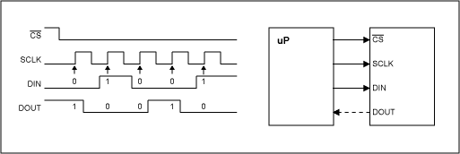
Figure
1. Signals and timing of the SPI-interface
Several devices might be connected to the
same bus, where all devices share the DIN and
SCLK-line. Each device has a separate
chip-select signal, so that the µP can address
the appropriate part by the relevant CS-bar
signal. If a chip does not talk back to the µP
(e.g., DAC), the DOUT-line is not needed. The
SPI-bus is well suited to data-rates to 20Mbps.
Some devices (e.g., RTCs like the MAX6901) have
a 3-wire interface, where the data-line is
bi-directional. This interface is similar to
SPI.
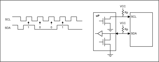
The I2C-bus has 2 signals: SCL =
Clock and SDA = Data in/out.
Figure 2 illustrates the timing of the
I2C-bus. Each device has a unique
7-bit or 10-bit address. As the data-line is
bi-directional, only 2 wires are required, which
is an advantage in space-constrained
applications or in designs where different parts
of the circuit have to be optically isolated.
Data-rates for the I2C-bus are
100kbps, 400kbps, or even µP to 3.4Mbps for the
high-speed mode. The I2C-bus requires
pull-up resistors Rp, where the value of Rp
depends on the supply-voltage and the
bus-capacitance (number of devices connected to
the bus and length of the bus).
Figure
2. Signals and timing of the
I2C-interface
If a system has different supply voltages for
the µP and for peripheral devices, suitable
level translators are required to be able to use
one of these serial interfaces. There are
several reasons why today's systems have two or
more supply-voltages. High-speed µPs and DSPs
are implemented on the most advanced processes
to get maximum performance with the lowest power
consumption. These processes are often limited
to supply voltages of 3V or less. Typical
core-voltages are 1.5V-2.5V. On the other hand,
I/O-devices like DA-and AD-converters might have
a supply-voltage of 3.3V or 5V to achieve the
required dynamic range. In portable and
low-power applications there is another reason
to have the µP run with the lowest possible
supply voltage. Current consumption of a typical
microprocessor depends on clock frequency and
supply voltage. One way to achieve low current
consumption is therefore to reduce the supply
voltage. This also leads to the situation where
the µP runs from a different supply than other
devices. Another reason for different supply
voltages might be the use of ASICs or FPGAs
together with a µP. For all these applications
the designer needs a uni-or bi-directional level
translator for the bus signals.
Figure 3 shows a basic level translator with
an N-channel MOSFET. If neither Q2 or Q3 pulls
the data-line low, VGS of Q1 is 0V and Data 1.8
has a level of 1.8V, Data 3.3 is at 3.3V. If Q2
pulls Data 1.8 low, VGS of Q1 is 1.8V and will
turn on Q1, pulling Data 3.3 low. If Q3 pulls
Data 3.3 low, the body diode of Q1 will be
forward-biased, pulling the source to 0.3V. VGS
will be 1.5V and Q1 will turn on, pulling Data
1.8 low. So logic-levels are translated in both
directions. We assume here that Q2 has zero
on-resistance. For a real application we would
have to consider this on-resistance, which is
133 worst-case for an I2C-compatible
output (0.4V at 3mA) or 22 for the 74LVC125
buffer (0.55V at 24mA). In this case the voltage
VGS to turn on Q1 would no longer be 1.8V, but
would be lower, depending on R1 and the
on-resistance of Q1.
worst-case for an I2C-compatible
output (0.4V at 3mA) or 22 for the 74LVC125
buffer (0.55V at 24mA). In this case the voltage
VGS to turn on Q1 would no longer be 1.8V, but
would be lower, depending on R1 and the
on-resistance of Q1.
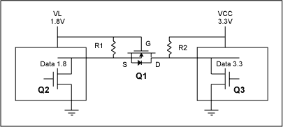
Figure
3. Basic level translator
There are several problems associated with
this circuit:
- With VL being 1.8V or even lower, the choice
of suitable MOSFETs with a low enough VGS
threshold voltage is rather limited. One
candidate might be the TN2501 from Supertex.
- The slew-rate and, therefore, the maximum
transmission rate depends on the value of R1/R2
and on the number of devices on the bus, which
determines the capacitance. It is possible to
increase the maximum transmission rate by
choosing lower value resistors R1/R2. This will
lead to higher current consumption, which is
undesirable in portable/low-power applications.
- With this simple circuit it is not possible
to tristate the bus and disconnect R1/R2.
Therefore one cannot switch off segments of the
bus.
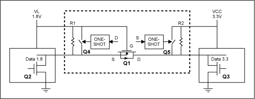
The MAX3372E-MAX3393E family of level
translators solves these problems. Figure 4
shows the simplified schematic of the MAX3373E,
where two MOSFETs Q4 and Q5 have been added. Q4
and Q5 close for a short time during the rising
edge and speed-up the low-to-high transition.
Minimum guaranteed data-rate for the MAX3373E is
8Mbps, µP to 16Mbps is possible if
|VCC - VL| < 0.8V. This
family of level-translators has a three-state
mode, where the pull-up resistors are
disconnected. This makes them ideal in
multidrop-networks or for controlling
I2C-devices with the same address,
where these devices are on different sections of
the network, which are decoupled by a level
translator.
The data-lines on the VCC-side are ±15kV
ESD-protected, which is a valuable feature in
applications where the bus is accessible on a
connector and where ESD-strikes are likely to
occur. A thermal-shutdown circuit puts these
level-translators in the three-state mode if
temperature exceeds 150°C.
Figure
4. Improved level translator MAX3373E with
speed-up circuit
Typical ApplicationsFigure 5 shows a
typical application for the MAX3390E level
translator in a battery-powered measurement
circuit. A MAX4194 low-power instrumentation
amplifier amplifies the signal from the bridge.
The signal is AD-converted by the MAX1270, a
12-bit 8 channel ADC. The supply voltage for the
analog front-end is 5V, the low-power µP has a
supply of 2.5V. The MAX3390E level shifts the
SPI signals from 2.5V to 5V and from 5V to 2.5V
for the DOUT signal.
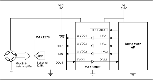
Figure
5. The MAX3390E level translator in an SPI-bus
application
Figure 6 shows a similar application with an
I2C-bus. The MAX3373E dual level
translator is used to interface the µP I/O
levels to the I2C-compatible
interface of the MAX1236 (4 channel 12 Bit ADC).
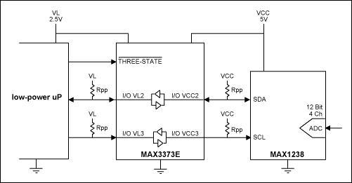
Figure
6. MAX3373E dual level translator used in an
IIC-bus application with optional pull-up
resistors Rpp
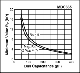
Depending on the number of devices on the
bus, optional pull-up resistors Rpp might be
required. The MAX3372E-MAX3393E family of level
translators has internal 10k pull-up
resistors. In Figure 7 we can see that this is
sufficient for a bus-capacitance of about 90pF,
assuming we do not connect the optional resistor
Rs (Rs=0). 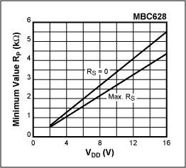
Figure
7. Maximum value of Rp as a function of bus
capacitance for a standard-mode
I2C-bus, from
I2C-specification
If there are several devices on the same bus
or if the bus is relatively long (>30cm), it
is necessary to use external pull-up resistors
Rpp. Figure 8 shows the minimum value of Rp,
which is 1.7k
for Rs=0 and VDD=5V. From this we find the
minimum value for Rpp to be 2.2k, so that Rpp in
parallel with the internal pull-up of 10k is 1.83k.
Figure
8. Minimum value of Rp as a function of supply
voltage with the value of Rs as a parameter,
from I2C-specification
In summary, the MAX3372E-MAX3393E are ideal
solutions to solve the I2C or SPI
bus-level translation problems found in
low-voltage systems. Guaranteed data rates, low
power requirements, low-supply-voltage
operability, and small packages help solve the
many problems facing designers in bus
architectures today.
AI2C™ is a trademark of Philips
Corps.
SPI™ is a trademark or Motorola Inc.
We Want Your
Feedback!
Love it? Hate it? Think it
could be better? Or just want to comment?
Please let us know—we act on customer
corrections and suggestions. Rate this page and provide
feedback.
| More Information |
|
APP 1159: Aug 05,
2002 |
| MAX1236 |
2.7V to 3.6V and 4.5V
to 5.5V, Low-Power, 4-/12-Channel, 2-Wire
Serial, 12-Bit ADCs |
Full
Data Sheet
(PDF, 408kB) |
Free
Samples |
| MAX1270 |
Multirange, +5V,
8-Channel, Serial 12-Bit ADCs |
Full
Data Sheet
(PDF, 824kB) |
Free
Samples |
| MAX3000E |
+1.2V to +5.5V, ±15kV
ESD-Protected, 0.1µA, 35Mbps, 8-Channel Level
Translators |
Full
Data Sheet
(PDF, 504kB) |
Free
Samples |
| MAX3372E |
±15kV ESD-Protected,
1µA, 16Mbps, Dual/Quad Low-Voltage Level
Translators in UCSP |
Full
Data Sheet
(PDF, 564kB) |
|
| MAX3373E |
±15kV ESD-Protected,
1µA, 16Mbps, Dual/Quad Low-Voltage Level
Translators in UCSP |
Full
Data Sheet
(PDF, 564kB) |
Free
Samples |
| MAX3390E |
±15kV ESD-Protected,
1µA, 16Mbps, Dual/Quad Low-Voltage Level
Translators in UCSP |
Full
Data Sheet
(PDF, 564kB) |
Free
Samples |
| MAX4194 |
Micropower,
Single-Supply, Rail-to-Rail, Precision
Instrumentation Amplifiers |
Full
Data Sheet
(PDF, 728kB) |
Free
Samples | |
|
 Download, PDF
Format (65kB) Download, PDF
Format (65kB)
AN1159, AN 1159, APP1159,
Appnote1159, Appnote 1159
| |